Efficient NAND analysis with AFM-in-SEM
Fault detection directly at the source

In modern semiconductor technology, troubleshooting in NAND memory chips is a challenging task. Traditional methods quickly reach their limits here - especially when it comes to precise, depth-resolved information on localised conductivity failures.
With LiteScope's AFM-in-SEM approach, these challenges can be solved directly in the analysis process - quickly, precisely and without sample contamination.
What is the problem with NAND error analysis?
NAND flash memory consists of complex, multi-layered structures. A fault in just one of these layers can lead to a complete malfunction. The central question when analysing is often:
Where exactly is the cause of a conductivity failure - and at what level of the structure?
To find this out, individual layers must be removed in a targeted manner and then analysed electrically. This is exactly where LiteScope comes in.
The solution: In-situ delayering and C-AFM measurement
With the LiteScope AFM-in-SEM system, the analysis can be performed without air contact and without moving the sample:
In-Situ Delayering

The workflow at a glance:
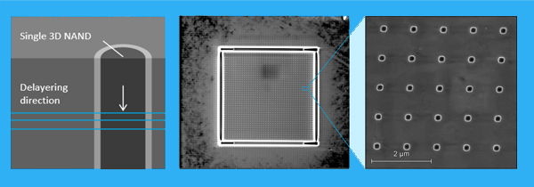
- Targeted delayering with PFIB
- Selective ablation of individual layers to defined depths (e.g. 5, 25, 50 nm ...)
- Precise control of transistors or vias - In-situ C-AFM measurement
- The contact-based measurement of the local electrical conductivity takes place directly afterwards
- No transfer, no oxidation, no loss of time - Result:
- High-resolution current maps
- I/V spectroscopy for in-depth analyses
- Causes of faults can be identified down to the individual level in the NAND
Why AFM-in-SEM for NAND analysis?
The combination of atomic force microscopy (AFM) and scanning electron microscopy (SEM) within one system offers decisive advantages:
Application relevance for industry, research and laboratories
Whether in production environments, in R&D or research laboratories, NAND defect analysis with LiteScope enables a new quality of nanoscale defect characterisation - even for complex or "invisible" defects that can no longer be detected using conventional methods.
The fully integrated AFM-in-SEM approach not only makes fault analysis more reliable but also measurably more efficient.
– Blog –


